

About Campus

Exploring the Development and Application of Modern Semiconductors, UNDIRA's Electrical Engineering Department Hosts Guest Lecture with Industry Practitioner


 By :
By : 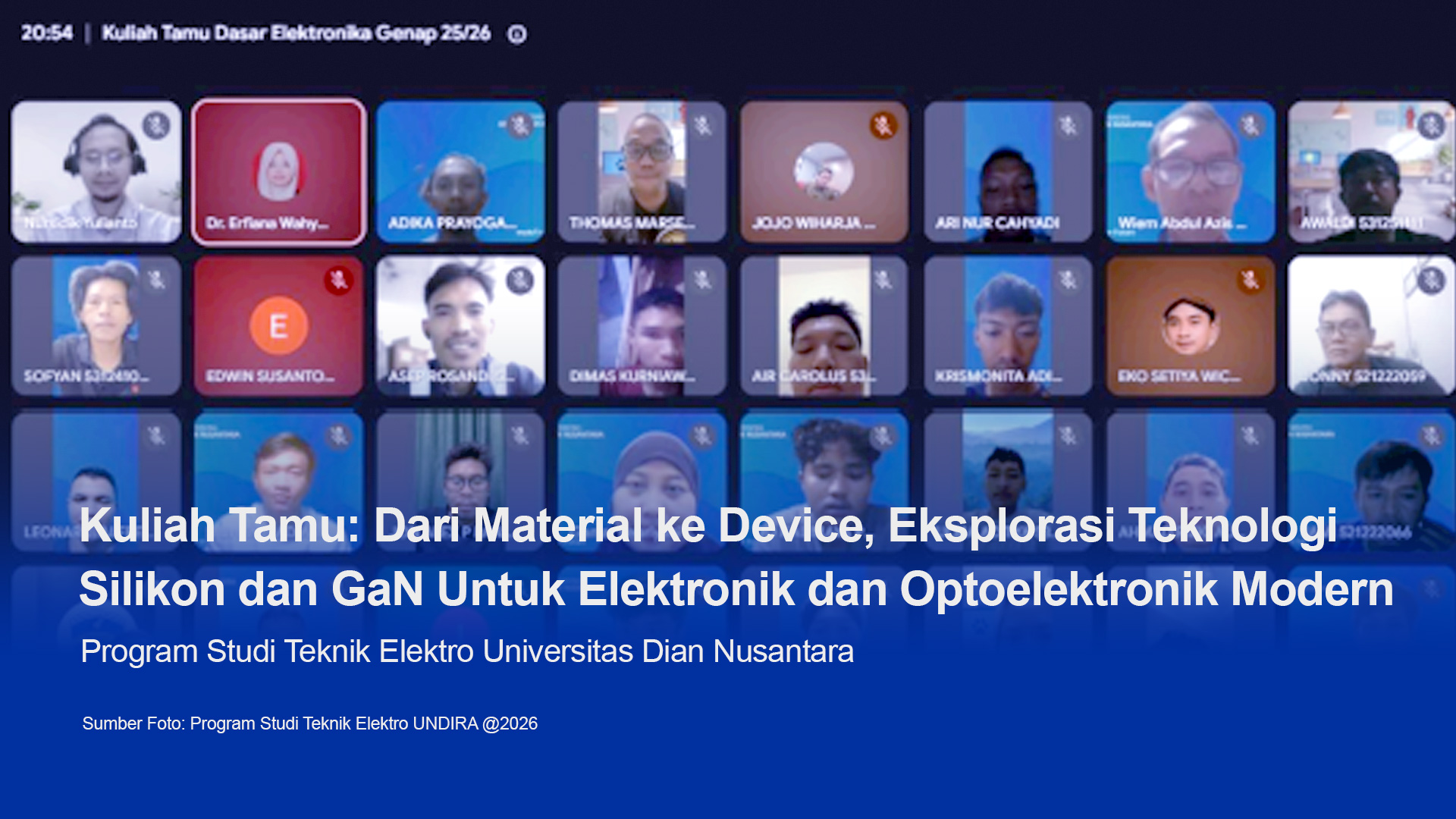
Jakarta, July 7, 2026 — Semiconductor materials have become the primary solution underpinning nearly the entirety of today's electronic and optoelectronic systems. As a material with tunable conductivity, semiconductors offer significant advantages by allowing precise control of electric current. Select materials such as silicon and gallium nitride (GaN) are considered capable of driving continued exploration in semiconductor development, particularly in terms of power efficiency and switching speed. This has made semiconductors a common base material for manufacturing chips and sensors across a wide range of electronic devices.
However, as with the broader strengthening of the materials and electronics industries, sustained innovation is needed amid the accelerating pace of technological change. In response to this challenge, the Electrical Engineering Study Program at Universitas Dian Nusantara (UNDIRA) held a guest lecture titled "From Material to Device: Exploring Silicon and GaN Technology for Modern Electronics and Optoelectronics."
Held online, the guest lecture drew enthusiastic participation from 101 students and featured Dr. Ing. Nursidik Yulianto, a photonics research practitioner from the National Research and Innovation Agency (BRIN), as the speaker.
In his opening remarks, the Head of UNDIRA's Electrical Engineering Study Program, Dr. Arie Pangesti Aji, stated that the guest lecture was expected to broaden students' understanding of the fundamental concepts of semiconductors as well as their applications in electronics.
"A deep understanding of semiconductors is not only about mastering the physics of the material itself, but also about how that material is applied into devices that genuinely benefit everyday life," he said.
Dr. Ing. Nursidik Yulianto outlined the long history of semiconductor technology, which has seen significant growth alongside rising demand for electronic devices across various sectors. Fundamentally, semiconductors rely on a "band gap" — the minimum energy threshold an electron must overcome to jump from the valence band to the conduction band, allowing electric current to be conducted.
He further explained that semiconductors are primarily built from silicon due to its ease of processing across industries and its abundant availability. Notably, Indonesia is one of the world's largest silicon contributors, with total reserves reaching 340 million tons circulated in the development of semiconductor-based industries and energy reserves.

That said, silicon is beginning to face challenges as the industry pushes toward smaller device sizes. As the channel length of silicon transistors continues to shrink to the nanometer scale, electrons tend to "leak" past the channel boundary, giving rise to a phenomenon known as current leakage. This leakage results in wasted energy and excessive heat generation, making it one of the key limitations of silicon in further miniaturization efforts.

Dr. Ing. Nursidik Yulianto also noted that when gallium reacts with an element from Group V, such as nitrogen or phosphorus, it can be processed into a semiconductor material through the formation of a III-V compound.
GaN offers a significant advantage in terms of its wide bandgap, enabling it to conduct electricity more efficiently and switch at much higher frequencies compared to silicon. According to him, this comes back to the fundamental concept of the High-Electron-Mobility Transistor (HEMT) layer and the two-dimensional electron gas (2DEG), which facilitate faster electron mobility and transfer across the band gap.
"GaN opens up major opportunities in the development of more compact and efficient power electronics, such as fast chargers, electric vehicle inverters, and power transmission systems. Beyond that, GaN also plays a role in optoelectronics, particularly in the development of light-emitting diodes (LEDs) and laser diodes, which are critical components in modern lighting technology and photonics-based optical communication," he said.
This guest lecture is expected to spark greater enthusiasm for learning among UNDIRA's Electrical Engineering students, while also opening the door to further research collaboration between UNDIRA and BRIN in the future. The event is also hoped to become a recurring initiative to enrich students' understanding of the ever-evolving landscape of materials technology and electronic devices in line with the demands of the global industry.
Press Contact :
Biro Humas & Sekretariat Universitas Dian Nusantara
Facebook : www.facebook.com/undiraofficial
Instagram : www.instagram.com/undiraofficial
Twitter : www.twitter.com/undiraofficial
www.undira.ac.id


Campus Tanjung Duren
Jln. Tanjung Duren Barat II No. 1
Grogol, Jakarta Barat. 11470
Campus Green Ville
JIn. Mangga XIV No. 3
Campus Cibubur
Jln. Rawa Dolar 65
Jatiranggon Kec. Jatisampurna, Bekasi. 17432
Campus Cibubur Kranggan Raya
Jln. Raya Kranggan, No.6, RT 006/ RW 008
Jatiranggon Kec. Jatisampurna, Bekasi. 17432


